Micro Switch 69SD5
Posted: 08 Jun 2020, 01:53
JP!'s recent finds had me taking another look at the SD boards that are sitting around here waiting to have something done with them.
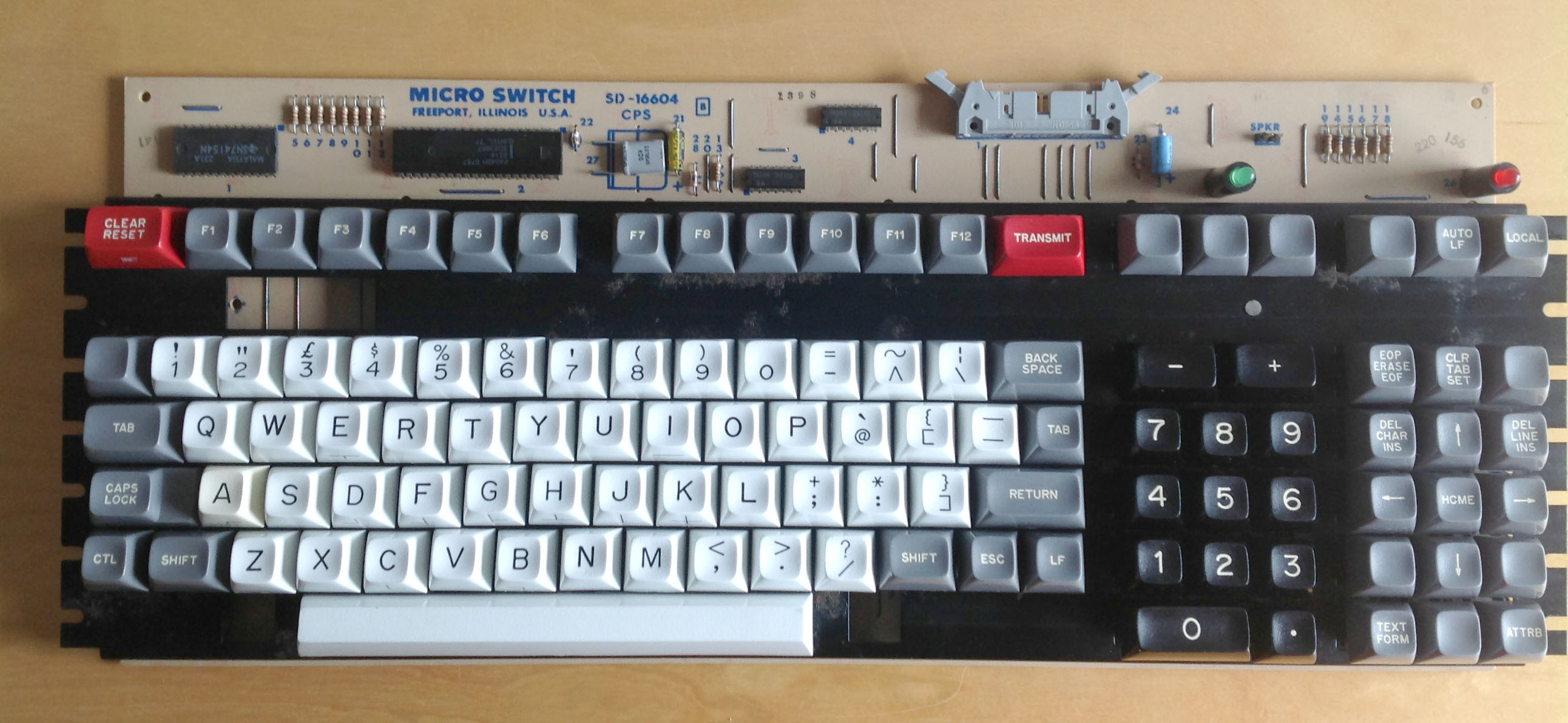
This board, 69SD5, is the guts of a data entry terminal for a Burroughs TD-730/830.
That is, it is more or less the same board as pr0ximity's in Burroughs TD016 "Data Preparation". Or the smaller sibling of another one here that still has its case, as discussed in Burroughs TD 830 Series Keyboard.
Specifically, it is the Latin American / Spanish variant.
Of course it's the same PCB, SD-16201. And while pr0ximity's is 69SD5-8-1, this is 69SD5-13-1. The date codes are 7811 and 7923, respectively. So I imagine the 13 is the key cap variation. And perhaps firmware, although the one here doesn't have its AMI LSI controller at all.
Some of the keys look like they got scratched by some through-hole pins or something and it has one replacement key cap. Though there is one just like it with the same date code but complete and undamaged on eBay right now for €200. So there's a cache of them out there.
The earlier topic didn't take a close look at the circuit.
The keyboard interfaced to the cable through a 2x15 PCB edge connector. The top side has +5V on the left two pins and then connections for its 12(!) LEDs, of which 8 are populated here. And the final pin is the other side of the LEDs' several 220Ω resistors. The missing 4 LEDs are also missing their common resistor.
The interface to the keyboard proper is on the other side. Two pins of ground, the dozen outputs of two hex inverters, and a connection to the last pin (28) of the controller.
The switch traces still have a bit of Chutes and Ladders that suggests not a matrix proper but two-of-n, like with SW series. And, indeed, almost all the switches are 4A3A. The beautiful baby blue command switches are a bit heavier and pulse only 4A8B.
The SHIFT LOCK is exactly that: the two SHIFT switches (61 and 48) and it (35) are all the same signal to the controller. These all have the dual outputs shorted together with a brief PCB trace.
Which leaves the strangest thing about the switch wiring. The RTAB (20) switch also has its outputs shorted. And it's a source level 4A3C and connected directly to one of the output inverters, skipping the controller. I cannot think of any reason to engineer it this way. Why would this function need special treatment?
I am almost inclined to believe that the PCB was designed for something else where this was some kind of attention key and reused for this terminal. Can anyone else think of something?
I am still debating what the best way to build a converter is, because of the need to access both the switch "matrix" from the MCU slot and the LEDs from the edge connector.
In a spot check, some of the keys didn't work. Every one of the scan lines got at least one hit, so it isn't a mistake there. May need to scope those switches and see whether they got damaged somewhere along the way.
This board, 69SD5, is the guts of a data entry terminal for a Burroughs TD-730/830.
- 69SD5-13-1-top.jpg (338.38 KiB) Viewed 5502 times
Specifically, it is the Latin American / Spanish variant.
- burroughs-td730-keyboard-specification.png (374.29 KiB) Viewed 5502 times
Some of the keys look like they got scratched by some through-hole pins or something and it has one replacement key cap. Though there is one just like it with the same date code but complete and undamaged on eBay right now for €200. So there's a cache of them out there.
The earlier topic didn't take a close look at the circuit.
The keyboard interfaced to the cable through a 2x15 PCB edge connector. The top side has +5V on the left two pins and then connections for its 12(!) LEDs, of which 8 are populated here. And the final pin is the other side of the LEDs' several 220Ω resistors. The missing 4 LEDs are also missing their common resistor.
The interface to the keyboard proper is on the other side. Two pins of ground, the dozen outputs of two hex inverters, and a connection to the last pin (28) of the controller.
- 69SD5-13-1-bottom.jpg (1.7 MiB) Viewed 5502 times
The SHIFT LOCK is exactly that: the two SHIFT switches (61 and 48) and it (35) are all the same signal to the controller. These all have the dual outputs shorted together with a brief PCB trace.
Which leaves the strangest thing about the switch wiring. The RTAB (20) switch also has its outputs shorted. And it's a source level 4A3C and connected directly to one of the output inverters, skipping the controller. I cannot think of any reason to engineer it this way. Why would this function need special treatment?
- burroughs-td730-keyboard-rtab.png (22.75 KiB) Viewed 5502 times
I am still debating what the best way to build a converter is, because of the need to access both the switch "matrix" from the MCU slot and the LEDs from the edge connector.
In a spot check, some of the keys didn't work. Every one of the scan lines got at least one hit, so it isn't a mistake there. May need to scope those switches and see whether they got damaged somewhere along the way.
- 69SD5-13-1-teensy.jpg (245.03 KiB) Viewed 5502 times