Page 1 of 1
IBM PC XT -> siXTyPerCent
Posted: 19 Jan 2016, 22:15
by tigpha
I'm thinking of chopping an IBM PC-XT into a 60% Model F. Something along the lines of this:

- siXTyPerCent-layout.jpeg (62.95 KiB) Viewed 6043 times
I plan to salvage the parts only from the PC-XT, and not rely on donor parts from other keyboards. The part that will take the most effort is the "logic board" design, which I'm sketching with no previous experience whatsoever in capacitive voodoo. Help! Can a kind engineer person look at what I've done so far, and put me right if I've done something silly?

- siXTyPerCent-v0.5.jpeg (281.84 KiB) Viewed 6043 times
I'm hoping to take further inspiration from the fascinating work done by Xwhatsit and the
xwhatsit's Grand Unified IBM Capsense USB controller thread.
I snatch a few hours every few days to work on this, so progress so far is slow, and probably will remain slow. I'll be very grateful for helpful comments and guidance.
Posted: 19 Jan 2016, 23:31
by Redmaus
Pretty sure this will require some sort of custom controller, whether that be xwhatsit or not.
Also, i'm not sure if chopping up a XT into this is the best way to achieve a homemade 60% F. Perhaps a F122 or almost any other F would make a better 60% keyboard.
Speaking from the heart, I have a hard time thinking anyone could permanently get used to having the function keys below the alphas.
Not sure if you have, but maybe checking out some of the XT threads already here and possibly the XTant project if you haven't already would help with an alternate solution that won't require any modifications to the outer case or the fabrication of another case.
A peek at Ellipse's kish reproductions may be your preferred choice as well. Do mind however, it is quite costly at 350$

Wish you luck

Posted: 20 Jan 2016, 12:43
by vivalarevolución
If you have any design abilities, perhaps you could adjust the files from the XTant project to work with a 60%?
workshop-f7/bringing-the-ibm-pc-xt-into ... 7-120.html
https://github.com/wcass-/XTant
On a related note, The Model M 60% has been done by a few people and it is document somewhere on DT and on geekhack.
Posted: 20 Jan 2016, 17:14
by idollar
Check this also: I am trying something similar
here, using information from the XTant. I you need help, do not hesitate to ask.
Posted: 20 Jan 2016, 19:32
by tigpha
Hi Redmaus, thanks for wishing me luck.
Thanks to i$ for offering help, I appreciate it. My help is on offer in return if needed.
I agree that a custom controller is needed, definitely. That's on the bill of work.
If I had a Model F122 battleship, I'd probably want to restore it and keep it in original shape, for bragging rights!
I'd love to own one, but shipping cost from the States is prohibitive -- they weigh six kilograms. "Jesus tap-dancing Christ!" As Chyros says in his review.
I was inspired to start this project because the PC-XT I recently bought is not in best condition. I might be salvageable, but I have two Bigfoots that I am perfectly happy with. The PC-XT would not get the same love, I'm not so enamoured with the design, so I decided to make something new out of it instead, resembling the Kishsaver.

The F1...F6 in the first image along the bottom aren't going to be function keys, necessarily. These are keys I have salvaged from the same donor. They happen to be the the darker ones that suit the aesthetic. The bottom keys are Meta, Alt, Space (9.75 units!) Alt-Gr, then some other Meta, Super, Ultra, Etc. These keys could be anything at all, since the controller will offer remapping and layers.
The Xtant and the XXI century PC-XT, and similar projects are my inspiration. These have given me confidence that at least others are just as nuts as I am, and have overcome problems that I expect to have.
The images I uploaded so far aren't very helpful. I'll supply better ones soon.
Posted: 21 Jan 2016, 22:16
by tigpha
Better images, as promised. These are not mirror images. The "under" image needs to be flipped, to be applied as an etching mask on a PCB. The prongs along the top are connection soldering pads for a ribbon cable. I haven't yet discovered a better connection method.

- sensor-pads-v0.7-over.png (163.17 KiB) Viewed 5922 times

- sensor-pads-v0.7-under.png (124.55 KiB) Viewed 5922 times
Posted: 23 Jan 2016, 14:20
by tigpha
Last night I examined the schematic that Xwhatsit very kindly published in his
IBM Capsense webpage
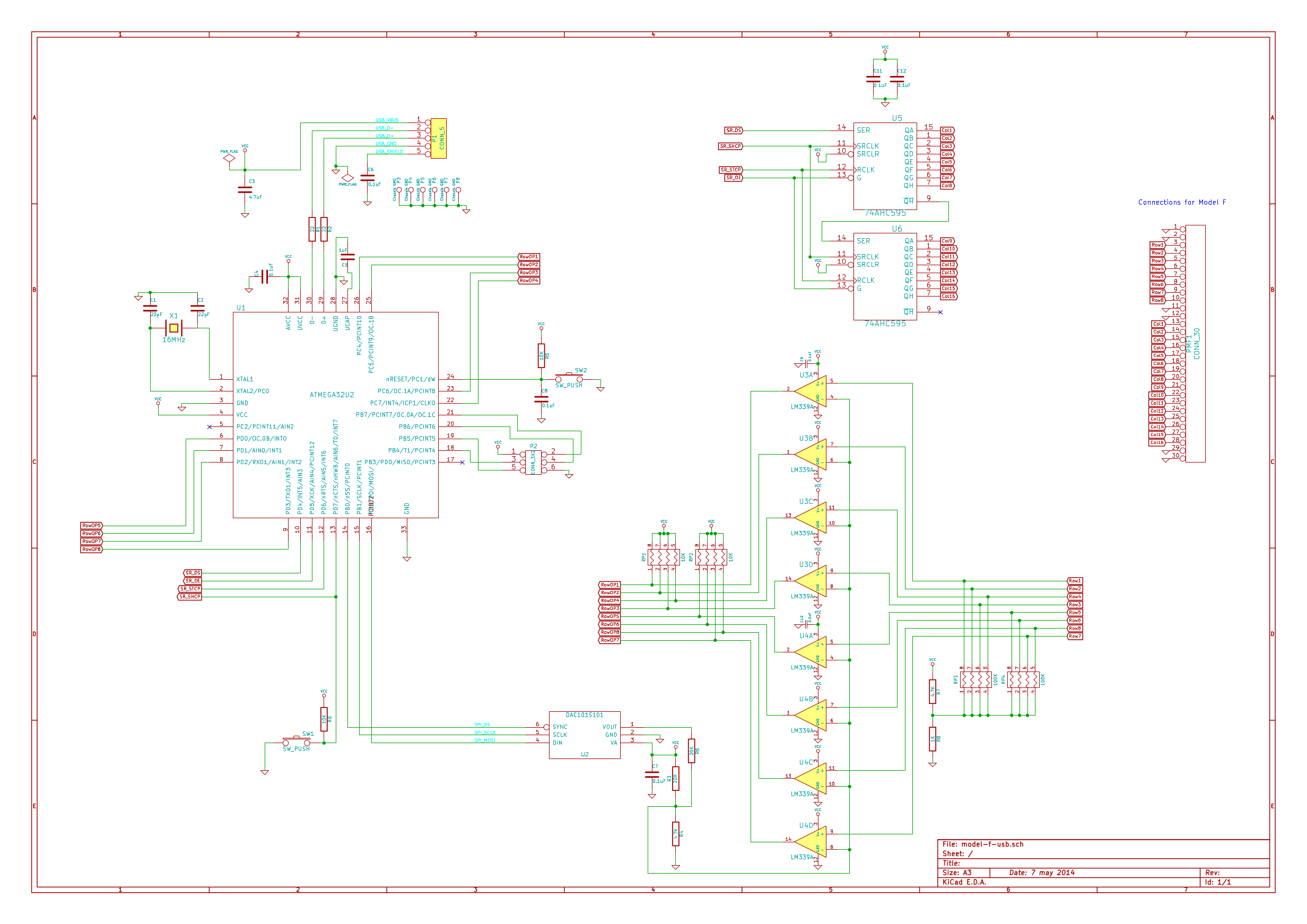
The circuit diagram needs no change, except perhaps omitting one of the 74595 8-bit shift registers, since the siXTyPerCent is an eight-squared matrix. The physical layout isn't practical for this project. I will need to draw up a more compact controller PCB, with the ribbon cable solder pads much closer together.
The software might not need any change at all, as I reckon that the key maps could be configured using the GUI utility programs which Xwhatsit includes in the project.
A big thank you to Xwhatsit for the detailed description on the webpage. It is greatly appreciated.
Posted: 23 Jan 2016, 15:04
by tigpha
The Xwhatsit controller PCB needs to be modified, to move the ribbon cable solder pads to the 0.05 inch pitch normally found these days, and to enable soldering the through via holes by hand. I'm trying to make the design as DIY friendly as I am able. Even though there are lots of PCB shops offering very small production runs to the general public, I've chosen to make the entire thing myself, by hand (I'm nuts...).
The original PCB layout includes via holes under the ATMEL chip. Soldering the via connections by hand might leave protrusions, blobs of solder that prevent the quad flat package from sitting onto the board surface. I have to move these via connections out from under the QFP.
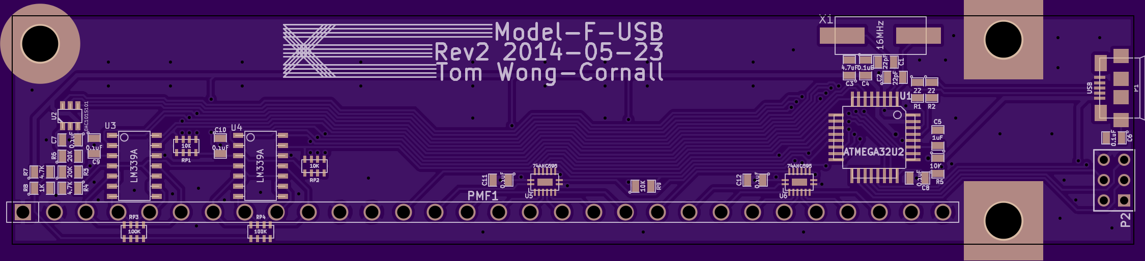
The size of the board is mainly due to the line of 30 connection holes along the bottom, required for the ribbon cable found in IBM Model F keyboards, and so that the controller PCB can benefit from the attachment screw positions in the existing cases. I think that I can shrink the board to half the size, even while spreading out the components to allow for hand assembly.
I searched for methods of creating through-connections on DIY PCBs. Most recommend threading wire and soldering either side. This is the simplest method which I choose to use. Another method is to cut copper wire into tiny rivets which are pressed to squash the ends flat against the copper sides of the board. The rivet method has a flatter profile which might lend itself better to via holes beneath QFP chips. It is very fiddly, and my patience would probably not stretch that far.
The most elaborate method of copper-plating via holes apparently originates from Russia. The DIY PCB makers deposit a very thin metallic copper coating to the insides of the via holes using a chemical method. The very thin layer of chemically deposited copper is built up by electroplating a thicker, more robust layer of copper on top. The holes have to be carefully drilled first, before etching the connecting traces, so that all the holes are electrically connected in the electroplating bath of copper sulphate solution. The
Russian Method only makes sense if production runs are big enough to justify the effort of preparing the chemical baths, and obtaining the oven necessary for baking the boards.
Another discovery is an improvement to the "toner-transfer" method of etching PCBs. It involves the use of "toner foil", after the copper plated boards have received the toner transfer treatment, and before etching. Toner foil is a very thin film of plastic, usually brightly coloured, sometimes with a metallic shine too, that is applied against the laser-printed toner fused to paper, or card, and then passed though the heated rollers of a laminator press. The foil sticks to the toner traces on the paper, leaving a coat of bright coloured foil on the areas covered with toner, but nowhere else. Some
clever persons realised that adding this foil to the toner transferred to PCB boards improves the result of etching, because the foil fills the pinholes and reinforces the areas that the printer did not cover so thickly.
I expect that toner-transfer + foil could be used for the silk-screen legend on the finished PCB too, to turn the black toner into a brighter colour such as white, perhaps.
Posted: 28 May 2016, 01:36
by DMA
oh wow. Just a week ago I've thought "why haven't anyone build 60% buckling spring keyboards yet?". And there you go. I was thinking about making the base flat though - just two flat pieces of metal and some bolts - because cutting metal is one thing, but cutting, slip rolling _and_ bending edges into shape afterwards seems a bit over the top for me. Also may be the plastic will suffice. Not sure.
This will, of course, require PCB rework (bolts will have to go thru PCB in several places, and they will be grounded). Will also try to make pads smaller (I think IBM made them a bit larger than absolutely needed). I have like 130 yards of 1/4"-wide copper foil with adhesive on the back - more than enough to experiment with the form of pads (may be even use the foil instead of etching - ghetto-style circuit boards, hehe).
Anyway, first step is the controller. I'm a bit surprised by amount of interest it got.
Posted: 14 Jun 2016, 08:37
by DMA
Playing with 122-key model F I've noticed that the rows which are close to each other have HUGE crosstalk. You want to keep them as far from each other as possible. Moving the trace towards those circles should be ok, but this NEEDS TESTING.
If you haven't made the PCB yet - I would seriously consider making the matrix 14x5 with a single sense between key rows + one under (that's "closer to the edge then") the spacebar or even some clever [15/16]x4 layout where rows don't even come close to the board edges. Will greatly improve signal quality.
Posted: 14 Jun 2016, 20:07
by tigpha
Hi DMA,
Thanks for sharing what you find. I don't quite understand, are you referring to the pairs of traces that run between the pads across the width of the keyboard? I meticulously copied the layout and spacings from an existing PC-XT PCB, and I haven't a clue if the result is electronically sound. I very much appreciate any guidance you can offer.
I'm going to review the PCB design soon. I have a minimalist design in mind which will need the exit pads relocated to a more top-and-centre position on the PCB. Making allowance for Real Life, I hope to share this here soon.
Posted: 14 Jun 2016, 21:43
by DMA
tigpha wrote: Hi DMA,
Thanks for sharing what you find. I don't quite understand, are you referring to the pairs of traces that run between the pads across the width of the keyboard? I meticulously copied the layout and spacings from an existing PC-XT PCB, and I haven't a clue if the result is electronically sound. I very much appreciate any guidance you can offer.
I'm going to review the PCB design soon. I have a minimalist design in mind which will need the exit pads relocated to a more top-and-centre position on the PCB. Making allowance for Real Life, I hope to share this here soon.
Yes, those. On the top of the keyboard, horizontally. You also want the part where those traces run parallel to each other, as short as possible. So, if not going for controller on the same PCB, I would move the interface top-right/top-left, with rows arriving to it from the same edge. If integrated - probably top-right is more preferred because LEDs are there.
Posted: 15 Jun 2016, 09:01
by tigpha
Ok, my simplistic understanding of your explanation is to avoid parallel lines (or surfaces, front to back) on the PCB where sensing is not supposed to happen. Because, capacitors! Of course
Would it help to insert a ground line between parallel lines on the PCB? What about ribbon cables? I suppose that these must be kept short, and that all sense/drive lines in the flat ribbon cable have to be interleaved with a ground line to separate them.
Posted: 15 Jun 2016, 11:00
by DMA
tigpha wrote: Ok, my simplistic understanding of your explanation is to avoid parallel lines (or surfaces, front to back) on the PCB where sensing is not supposed to happen. Because, capacitors! Of course
Unless you want them to talk to each other!
tigpha wrote:
Would it help to insert a ground line between parallel lines on the PCB? What about ribbon cables? I suppose that these must be kept short, and that all sense/drive lines in the flat ribbon cable have to be interleaved with a ground line to separate them.
Ground between rowlines will make parasitic capacitance greater - so the signal will be weaker.
I know a much better thing to put between them, though: sense pads/keys.
like
[q][w][e][r][t][y]
--------------------- <= that's one row trace.
[a]
[d][f][g][h]
--------------------- <= that's another
[z][x][c][v][n]
This way you should be able to cram the matrix into 16x4.
Ribbon cables is a necessary evil. Just keep the parallel runs to a minimum - it's not feasible to completely eliminate them.
If you manage to make a better than needed job at reducing parasitic capacitance though and can't figure out the key states because the signal is equally strong in both states - interleaving the sense lines with ground at ribbon cable level will help with that.
Posted: 15 Jun 2016, 14:16
by tigpha
To illustrate, I suppose something resembling the beamspring PCB, such as the one shown in the
Rustmaster Strikes Again!. I'll aim to design the matrix as a four-by-sixteen grid. The PSoC 5 series appears to have enough I/O to cope with that, without need for external components. In fact, with 72 I/O, the matrix grid could even be 71 x 1, but that requires too many wires!

Posted: 15 Jun 2016, 16:59
by DMA
So I've reinvented IBM's wheel.
That's a good thing!
But yes, I've meant exactly that.
Posted: 15 Jun 2016, 19:23
by tigpha
The beamspring design gets lots of praise in DT fora. Probably because they are massively over-engineered, built according to exacting principles. It is curious to note that the parallel sense/drive lines is a modification made later, possibly by IBM engineers who where satisfied with "good enough" and didn't mind cross-talk, or didn't fully absorb the meaning and intention of the original design and were lucky that they didn't compromise the result.
Posted: 15 Jun 2016, 19:55
by DMA
tigpha wrote: The beamspring design gets lots of praise in DT fora. Probably because they are massively over-engineered, built according to exacting principles. It is curious to note that the parallel sense/drive lines is a modification made later, possibly by IBM engineers who where satisfied with "good enough" and didn't mind cross-talk, or didn't fully absorb the meaning and intention of the original design and were lucky that they didn't compromise the result.
I think it was because they tried to cram them into the space that's occupied by the border of the barrel.
You see, the beamspring key seem to just disappear, while model F flipper has one side of it sitting firmly on the ground.
When I'm done with the initial version of the controller (I'm close, basically just need to move config back and forth between device RAM and EEPROM), it will be time to experiment with sense pad design. I will be able to answer this question after those experiments. I already have like 200 yards of quarter-inch copper tape for rabid prototyping.
Posted: 19 Jun 2016, 21:52
by tigpha
New PBC design, following suggestions from DMA. First the rows, on the front of the PCB:

- sensor-pads-v0.8-2016-06-18-rows-B&W.png (43.99 KiB) Viewed 5626 times
And the columns, on the back of the PCB:

- sensor-pads-v0.8-2016-06-18-columns-B&W.png (40.67 KiB) Viewed 5626 times
The weird lines leading nowhere are ground lines to prevent cross-talk. The connections are by 0.05 inch pitch ribbon cable to the controller, which looks as if it will be a PSoC from Cypress.
The matrix is nine-by-seven, divided into two halves left and right of the PCB (above and below in the images).
Posted: 19 Jun 2016, 22:17
by DMA
top row sense line looks perilously close to that solid column ground plane.
This will bite - the signal from the top line will have lower amplitude. But how much exactly - I do not know. It should be possible to retrace it to 4/8 rows. And if it's 8 rows - are you going to connect 2 columns to the same pin on the controller? Wouldn't it complicate the cabling?
Also I've discovered the calibration pad on my F122. Don't know how they made it, though. Afraid to disassemble it - the foam looks reeeeally decomposed.
Posted: 20 Jun 2016, 22:06
by tigpha
More PCB revisions.
Composite view with colour coded rows and columns:

- sensor-pads-v0.8-2016-06-18.png (38.19 KiB) Viewed 5596 times
The columns on the under side of the PCB, which appear to be the driven lines on the IBM PC-XT reference. The columns are separated by chunky ground fencing, which I guess is necessary because these lines will carry relatively high voltages, and need protection from cross-talk:

- sensor-pads-v0.8-2016-06-18-columns-B&W.png (18.54 KiB) Viewed 5596 times
The rows on the upper side of the PCB, which appear to be the sense lines on the IBM PC-XT reference. I have moved the sense lines away from any ground planes, but I still have the interleaved ground lines separating the sense lines to avoid cross-talk. I'm not sure how critical this is on the sense lines as the voltages will be very small -- the interleaved ground lines might suppress the sensed signal by capacitive coupling to ground.:

- sensor-pads-v0.8-2016-06-18-rows-B&W.png (16.47 KiB) Viewed 5596 times
DMA, the sense lines on the original PC-XT and Bigfoot terminal keyboards do not have interleaved ground lines, but there are large ground planes beneath the sense lines leading up to the controller circuit. Do you reckon that the interleaved ground lines on the last image are actually of any use?
Posted: 20 Jun 2016, 22:12
by tigpha
DMA wrote: top row sense line looks perilously close to that solid column ground plane.
This will bite - the signal from the top line will have lower amplitude. But how much exactly - I do not know. It should be possible to retrace it to 4/8 rows. And if it's 8 rows - are you going to connect 2 columns to the same pin on the controller? Wouldn't it complicate the cabling?
I moved the sense lines away from the ground planes.
DMA wrote: Also I've discovered the calibration pad on my F122. Don't know how they made it, though. Afraid to disassemble it - the foam looks reeeeally decomposed.
I've not found sense pads on the IBM Bigfoots, or the PC-XT, but maybe I didn't know what to look for. As for the foam,
I replaced this with 2mm thick neoprene foam. It was a minor struggle, but I believe it was well worth the effort.
Posted: 20 Jun 2016, 22:29
by DMA
DMA wrote: Also I've discovered the calibration pad on my F122. Don't know how they made it, though. Afraid to disassemble it - the foam looks reeeeally decomposed.
I've not found sense pads on the IBM Bigfoots, or the PC-XT, but maybe I didn't know what to look for. As for the foam,
I replaced this with 2mm thick neoprene foam. It was a minor struggle, but I believe it was well worth the effort.[/quote]
It's not much of the effort - but I need to get controller going first.
I'm also not sure anymore about how much ground should be around the sense traces - see the update on controller post, the input is really, really strange. I have an idea why (i'm going too fast to the next column and sense lines don't have time to fully discharge), but need to test it.