Page 3 of 4

Posted: 07 Feb 2016, 14:37
by XMIT
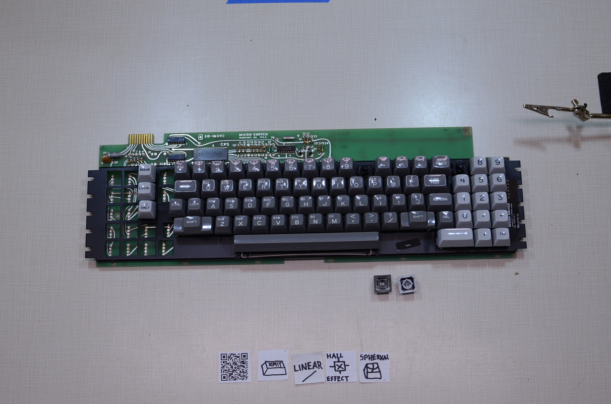
As implemented, this board is only capable of 1KRO. I'm working on wiring a 2x2 matrix of Hall sensors for firmware testing.

There are some tricks for possible NKRO support that I'll get to later but I think all of them will require a new PCB. I'm working on a 1KRO solution that is an easy enough retrofit for anyone with one of these boards today, and may or may not get to designing a new PCB.

I've been playing with EAGLE some. Here is a schematic for a 2x2 matrix of these Hall switches.
2016-02-07_1115x748.png
2016-02-07_1115x748.png (29.78 KiB) Viewed 11716 times
This small example is exactly how the switches on the board are wired (though the resistor value may be off; that doesn't matter). There is one pull up resistor per row and one pull up resistor per column. When a switch is pressed, it pulls its row and its column, from high to low, for 60µs ± 3µs. The precision here is pretty good.

Now consider what happens if A (upper left - row 1, column 1) and D (lower right - row 2, column 2) are pressed at exactly the same time. For 60µs, all of row 1, row 2, column 1, and column 2 are low. There is absolutely no way to determine if the user has pressed AD, BC, ABC, ACD, BCD, ABD, or ABCD. Since there is no way to tell the only sensible thing for the keyboard firmware to do is to toss away the result and act as if no key was pressed. This is easy to detect by AND'ing together the results of all the column scans for which a row was pressed, and blocking if the result AND's to something other than zero.

In pseudocode this might look like:

Code: Select all

#define NUM_ROWS 6
/* Holds results of one pass of matrix scan. Use high bit to note that row was set. */
uint32_t sense[NUM_ROWS];
uint32_t block;
uint8_t i, row;

/* Main scanning loop. */
while(1) {
for(i=0; i<NUM_ROWS; i++)
{
    block = 0;
    /* Reads row i of sense matrix. Lower bits are set if columns are set. High bit is set if row is set. */
    sense[i] = read_row(i);
    block &= sense[i];
}
if(block) break;
/* Continue keyboard sensing. */
}
For sensing, I can take advantage of the fact that the pulse width is almost exactly 60µs wide consistently. So long as I scan the entire matrix every 30µs - that works out to 33 ⅓ kHz - I can read the pin value directly. There are six rows, so I could switch between rows every 5µs.

Of course this only blocks when two switches are pressed together (or in an overlapping fashion that triggers the blocking logic). With a 60µs pulse width the chances of this happening are vanishingly small - perhaps this is why the Micro USA engineers chose this width. But the chance must not be dismissed.

Now, back to those aforementioned tricks. There are two that come to mind:

1. Use the output of a Hall sensor to drive the gate of a FET. Then, use the FET itself as a regular old switch with a diode across it, and scan this as if it were an array of mechanical switches. This would give NKRO.

2. Wire every Hall switch to its own pull up resistor and select between these through one or more multiplexers. Then I'm able to detect individual switches. The existing board sort of does this but is still limited to 1KRO because of the shared row and column sense lines.

Both of these techniques work with "hold low" and "pulse low" switches. In the case of the former you'd have true NKRO since you know when presses are pressed and released. For the latter, you still only get press events from the hardware but at least you can detect the presses without blocking.

A while ago HaaTa proposed a solution involving strobing the power lines to achieve NKRO. I worry about this proposal. For one, I don't know how the Hall hardware would respond to being driven with a 33kHz square wave. For two, I don't know how these switches are calibrated - either with a fixed factory calibration or a dynamic power on calibration. It's possible that rapid power cycling would throw off the calibration. Three, I don't know what sort of delay the switch gives between power on and being able to sense; we may not be able to strobe power fast enough.

Fun times.

Posted: 10 Feb 2016, 18:45
by XMIT
Quick update: I've decided that TMK is the best fit for prototyping a single switch and a 2x2 matrix given my preference for cheap ATmega32u4 based boards (sorry HaaTa).

For now, my controller will require a substantial rework to access the row and column sense pins on the keyboard directly. If there is time and interest I'll work to simply attach to the existing wire (using the board's 7400 series AND logic) so no rework is necessary.

Posted: 11 Feb 2016, 13:32
by snuci
I think I have some interesting information that can help but I had no idea you guys were working on converting a hall-effect keyboard to USB from this thread title. @Firebolt1914, would you consider changing the title of this thread so others might find it? Perhaps "Converting Hall-effect keyboards to USB" ? The information here is not about the Wang keyboard specifically so I was hesitant to post it in this thread.

Anyway, I pointed out one of the hall-effect Micro Switch keyboards I have in another thread. It is my "home made keyboard" that is a serial or parallel ASCII keyboard cobbled together from parts from a Diablo Hyterm paper-based terminal. The parts used were the main processing board and the Micro Switch keyboard but unfortunately, I don't know much about it and I can't get it to work.

My keyboard: http://vintagecomputer.ca/vintage-homemade-keyboard/

The Diablo Hyterm terminal: http://www.columbia.edu/cu/computinghistory/diablo.html

What I also have is the paper schematics used by the original owner to put this together. I have scanned them.

Schematics are here: http://vintagecomputer.ca/?wpdmdl=142

Further information is on Bitsavers in a Diablo Hyterm Maintenance manual here: http://bitsavers.informatik.uni-stuttga ... _Dec78.pdf

I think this may even have my schematics in it but the key is that I have the exact matching keyboard and we have the full schematics and the encoding chart on (see Section 2.10 in the Hypterm Maintenance Manual.

Sounds like you guys are starting at ground zero. I think the information on my Diablo Hyterm keyboard will help.

Edit: One thing I forgot to mention. This Diablo Hyterm also can use a keyboard based on saturable-core keyswitches (Cortron). Might be interesting for converting those?

Posted: 11 Feb 2016, 13:46
by XMIT
Thanks so much for sharing that schematic! This looks just like my board. The keys are specified to have 50us low pulses and the modifiers hold low. Matrix reading is done through a multiplexer. There is no controller in sight and column sense pins seem to go out over the wire. With some minor modifications whatever I manage to get working with my board will work with this one.

I hope the thread title changes too but I cannot fix that. If the OP doesn't get to it maybe Muirium or someone can do it.

I've been reading through the TMK source and the ATmega32u4 data sheet and am starting to have an idea of the modifications I need to make. First I will get one switch working! Then I will wire in a small matrix. Then the full board.

Posted: 11 Feb 2016, 16:08
by XMIT
Oh, weird, I think I just happen to have a Diablo Hyterm keyboard module here. I paid what I think to be too much for it but it's brand new. I pulled the "UC ONLY" key from it earlier in this thread for some investigation work.

Image

(Oh the benefits of having a full online catalog. I really need to re-do my inventory.)

I'll get to ITW/Cortron switches later. Many of those have actual controllers so it's a simple matter of protocol conversion. It should be possible to sense them just like a regular key switch with pulses. They are already debounced because the "reflected" pulse that comes out of each switch is shrunk. After it goes through more than one switch it's basically not readable as a logic level. At least that's my understanding, I'll need to look at it some more.

Posted: 15 Feb 2016, 18:26
by XMIT
I had a chance to look at the power on behavior of two switch types: 4A2K, which emits a low pulse when pressed, and 4B3A, which holds low when pressed. The purpose of these experiments was to determine if power strobing is an effective way to deal with these low-pulse switches.

In these diagrams, the yellow (top) channel is the sensor output (e.g. where the output pin meets the pull up resistor) and the green (bottom) channel is power. I triggered to rising power, held the key switch down, and flipped the power supply switch on in both cases

First, the 4A2K, low pulse:
20160154_hall_effect_single_pulse_power_on_capture.png
20160154_hall_effect_single_pulse_power_on_capture.png (99.78 KiB) Viewed 11634 times
About 1-2ms after power on, when voltage reaches some critical level, the switch becomes active. The low pulse is present but extremely noisy. Afterward, voltage continues to rise.

Second, 4B3A, the "hold low" switch:
20160154_hall_effect_continuous_low_power_on_capture.png
20160154_hall_effect_continuous_low_power_on_capture.png (96.2 KiB) Viewed 11634 times
This switch takes 1.79 ms to "settle" after some power on bounce and then outputs a continuous low signal.

In both cases, the low bounces are absent if a key switch is not depressed as I power it on (if there is no magnet next to the sensor).

Conclusions:

Power on strobing may be effective and would add NKRO capabilities (since we can detect switches independently *and* detect if a switch is powered on at a granularity of about 500Hz) but will certainly add complication to the board.

For the "pulse low" switches: it is best to sample about 1.5ms after power on and see if the voltage level ever achieves a "low" state.

For the "hold low" switches: I can sample 2ms after power on to see if the switch is depressed.

The "hold low" switches are vastly preferable in all regards except power consumption (current is flowing through the pull up resistor when the key switch is pressed). However they seem to be uncommon, and reserved for modifier keys.

What this means: for now, I'll focus my efforts on regular matrix scanning, and save power strobing to a much later stage. It would almost certainly require a PCB and some fast, clean MOS switches to implement well.

Posted: 23 Feb 2016, 08:41
by Halvar
I became curious yesterday and did some quick measurements on my little Micro Switch keyboard. I only have a multimeter, no logic analyser or scope, and I also didn't want to solder out components just yet.

I connected the keyboard to some batteries (4.5 V) and looked what happened when I pressed a key (without taking out the switch). What happened on all keys was that the 2 sense lines were both drawn to low for the whole time while the key was pressed. They only went back to high when the keys were released.

For me, that seems pretty nice, because if the matrix is laid out in a sensible way I think that should be enough for 2KRO with keydown and keyup detection in the case of this keyboard, by just replacing the decoder IC with a TMK'd Teensy. All modifiers are on separate lines outside the matrix anyway, so 2KRO should not be a huge problem. I didn't look at power consumption yet though.

Am I missing something?

Does anyone know what these little white ceramic cylindric things on the second picture could be? For my multimeter, they look like pure wires, no resistance in any direction when measured while inside the circuit (and there are no parallel traces). Electronically, they are located between each switch sense line (i.e. row and column) and its controller input pin. They have no markings whatsoever. I wonder if they could be voltage limiters maybe, but I have no idea.
IMG_20160222_193420.jpg
IMG_20160222_193420.jpg (130.48 KiB) Viewed 11601 times
IMG_20160222_193927.jpg
IMG_20160222_193927.jpg (175.83 KiB) Viewed 11601 times
IMG_20160222_193938.jpg
IMG_20160222_193938.jpg (122.38 KiB) Viewed 11601 times
IMG_20160222_194249.jpg
IMG_20160222_194249.jpg (304.78 KiB) Viewed 11601 times

Posted: 23 Feb 2016, 15:57
by Firebolt1914
Could the Wang board have certain switches that don't hold for the sake of the solenoid? I'm just making speculations without understanding how the board works. :p

Posted: 23 Feb 2016, 16:18
by XMIT
Firebolt1914 wrote: Could the Wang board have certain switches that don't hold for the sake of the solenoid? I'm just making speculations without understanding how the board works. :p
Image

Seriously, though, the solenoid circuitry is independent from all the switches. This is connected to a terminal that can presumably provide all the power needed. The switch choice was just an odd design decision. :roll:

Posted: 23 Feb 2016, 16:21
by XMIT
Great reply, Halvar, thanks. Your board should be easy to sense using TMK (modified for low instead of high sense). You don't need to strobe at all - you would sense on both rows and columns.

Could you please provide a few more photos? In particular:
  • Rear of board, showing traces;
  • Underneath key cap, showing switch code (4 or 5 characters) and PCB mount style;
  • Detail of any discrete components or integrated circuits (chips) above the switch plate;
  • Side profile (for fun - wondering if these are sculpted).
As for your question of what the white things are: I suspect they are "zero ohm resistors" but they could be inductors. I'm not sure.

Posted: 23 Feb 2016, 16:55
by Halvar
Thanks for your help XMIT, yes, that's what I thought, too, about sensing rows and columns with TMK. I will have to figure out the matrix next, which seems in fact to have some peculiarities...

I will post more photos and add values later. The components on the board are:
  • AMI 8544MAB encoder/decoder/controller or whatever that's called. I found no information at all on this chip.
  • 4 x DM7400N, each of them containing 4 NAND-Gates. Most of these are used as simple inverters on output signals of the main chip, some seem to work on the output signals in a way that I haven't fully traced yet.
  • 9 pullup resistors (3,0 kOhm) on the output signals of the main chip
  • 4 pullup resistors (6,8 kOhm) on the modifier switch sense signals
  • electrolyte capacitor 15 µF between Vcc and GND, diode as a fuse (? or whatever that is) between Vcc and GND.
  • 12 mystery "0 Ohm resistors".
EDIT: added resistor values

Posted: 23 Feb 2016, 20:05
by Slom
Halvar wrote: Does anyone know what these little white ceramic cylindric things on the second picture could be? For my multimeter, they look like pure wires, no resistance in any direction when measured while inside the circuit (and there are no parallel traces). Electronically, they are located between each switch sense line (i.e. row and column) and its controller input pin. They have no markings whatsoever. I wonder if they could be voltage limiters maybe, but I have no idea.
My board has the same PCB as yours, but I have different connections there. Maybe this is to accommodate different layouts.
XMIT wrote: [*] Rear of board, showing traces;
Has anybody ever thought of using image manipulation to get the matrix from a photo of the PCB?
XMIT wrote: [*] Underneath key cap, showing switch code (4 or 5 characters) and PCB mount style;
my switches are all 4A3A
XMIT wrote: [*] Side profile (for fun - wondering if these are sculpted).
Mine are not sculpted, as you know.

Posted: 23 Feb 2016, 21:41
by XMIT
Ah. 4A3A and 4B3A are both variants of "hold low" switches, as opposed to 4A2K which is a "pulse low" variant.

The reason that comes to mind for not making a board of these is: when they are held low, current is flowing through the pull up resistor. But even so, i you were to press every switch on the board you'd have 5V / 10k ohm * 100 = 0.05A of current. That's well within the 500mA power budget of USB.

So, Halvar and Slom, you will probably have working Hall boards before I do.

Posted: 24 Feb 2016, 01:18
by Halvar
Yes, 4A3A are the ones on mine, too.
Switches
Switches
P1010231.JPG (352.85 KiB) Viewed 11520 times
Backside of PCB
Backside of PCB
P1010236.JPG (428.72 KiB) Viewed 11520 times
Type label
Type label
IMG_20160222_193955.jpg (412.37 KiB) Viewed 11520 times
Logic chips
Logic chips
IMG_20160222_193917.jpg (368.9 KiB) Viewed 11520 times
Yeah, whatever ...
Yeah, whatever ...
P1010251.JPG (257.75 KiB) Viewed 11520 times
I forgot the side photo of the keycaps, but they're flat anyway, not sculpted.

Posted: 27 Feb 2016, 23:31
by Halvar
I'll quote a different thread here, but I think my response belongs here:
XMIT wrote:
Muirium wrote: So I guess [NKRO is] possible. But maybe only by sawing off the original controller.
Yes. With some effort the switches support NKRO. I have not seen a PCB and/or controller for Honeywell switches that does.
I thought about how to do this today because I'm trying to convert my Micro Switch board, that only has the "hold low" switches.

Like XMIT already found out for his board, with the kind of "matrix" this thing has, you can only get 1KRO! :(

Basically you have two digital outputs on each switch that are both "high" while the switch is off, and "low" while the switch is pressed. These switches are wired to a number of (in my case 13) input pins on the controller in such a way that every key has a different combination of exactly two input pins being on low when it is pressed. There is no scanning, and there aren't even discernible row and column pins!

Modifer keys are outside the matrix on extra pins but let's ignore those here.

So if one matrix key is pressed it can be identified correctly by the combination of two pins {a,b} being on low. (I'm writing this as a set because it's just a combination of two pins on the controller. {a,b} and {b,a} are the same)

Now if a second key is pressed with the first one still held down, there are two cases, we can be either lucky or less lucky: if were're lucky, the new key is on two different input pins than the first one. If we still know what the first key was, we can identify the second key if we assume that no more than one key changes from cycle to cycle, which should be ok if the cycles are short enough.

If we're less lucky, the second key shares one controller pin with the first key. Then we have three pins on low, and we know which two of them belong to the first key. So the new third pin belongs to the new key, so much is clear. But we don't know which one of the other two pins belongs to the second key! So we can't tell what the second key is.

Example from my board:
{1,2} is the key "1!" on the num row. Let's say this key is pressed first. The controller sees pins 1 and 2 on low and knows that the key being pressed is the "1!" key.

Then I press a second key. The controller now sees that {1,2,5} are on low, and it can't decide if I pressed the key on {1,5} which would be the "4$" key on num row, or the key on {2,5} which would be the "Q" key.

So it's really 1KRO, and I think it won't be fun to type fast on this thing, because whenever you hit a new key before having released the previous key, you risk that the new key can't be identified...

The reason for that is that the "matrix" on this board isn't really a matrix in the sense we know from scanning boards. There are no two disjunct sets of pins on the controller that can be called "rows" and "columns" respectively. The designer of this board crammed 47 keys on 13 encoder pins, which wouldn't be possible with a scanning matrix, because 13 pins can identify no more than 6*7 = 42 keys on a scanning matrix.

If they had used 14 sense pins, they could have used a 7x7 matrix, and 2KRO would have been possible, because every pin would be known to the controller to belong to either a row or a column, so if a second key is pressed, the controller can know whether it is on the same row or the same column as the first key.

So now I know I will have to rewire the matrix in order to get 2KRO.

Food for thought: Can I get 3KRO? If it's possible, how many GPIOs do I need? My intuition says we'd need more sense pins per switch, but it's late and I had some beer...

Is it even possible to get NKRO, without having as many controller pins as we have keys, and without using much more components? I'm fine with not being able to detect more than one change happening in one scan cycle.


EDIT:
Power consumption: 110 mA at 4.2 V with no keys pressed, goes up to 180 mA when all 53 keys are pressed. So USB should not be a problem for this little keyboard.

Pinout of the PCB edge connector:
Here it really bites me that I can't find any information on the AMI 8544MAB Encoder chip and I have no logic analyzer.

Bottom side (soldering side), pins 1 to 12:
1: GND
2: Vcc
3: n/c
4,5,6,7,10,11: inverted pulled up (3K) outputs from the encoder chip (pins 15 to 20 on the encoder chip). Speculation: data pins 0-5
8: n/c
9: a logical combination of two encoder output pins (21,23) and the state of the CONTROL key. Speculation: Data pin 6
12: output pin 24 of the controller, doubly inverted. No idea what this is for. Maybe strobe signal?

Top side (keys side), pins A to L:
A: Signal +5V. This is an output of the decoder chip, all pullups on the output side are pulling up to this. Not directly connected to VCC, but when I power the board, this goes up to U = Vcc.
B: n/c
C,D,E,F: not connected to anything on my board, but they could be connected to special keys with a different setup of jumpers on the same PCB.
G: sense pin of the "Start" key switch, pulled up with 6.6 kOhm
H: sense pin of the "Up Shift" key switch, pulled up with 6.6 kOhm
I: sense pin of the "Break" key switch, pulled up with 6.6 kOhm
J: sense pin of the "Start" key switch, pulled up with 6.6 kOhm
K: n/c
L: sense pins of both "Shift" key switches (low when either is pressed)

Posted: 28 Feb 2016, 15:54
by Halvar
Micro Switch SD-16127

To conclude this, here are the (part) schematics I drew up, and the matrix. I don't know if that will ever help anybody, but maybe it's a start if you have something similar.

The matrix isn't a keyboard matrix as you know it. It's just my way of writing up the individual two pins that each switch is connected to. Numbers in the matrix are switch numbers as they appear on the PCB.

I'm not sure yet what to do with this board. Due to its simple layout and the 1KRO, I'm not sure if I would use it very much, so I feel hesitant at the moment to really destroy its current self by soldering out the encoder IC, and there's also the question of the missing enclosure (I only have the barebone). Maybe I'd rather go on by trying to find out if I can make a converter, with all the limitations that would have.

Posted: 28 Feb 2016, 17:03
by Slom
Halvar wrote: Micro Switch SD-16127

To conclude this, here are the (part) schematics I drew up, and the matrix. I don't know if that will ever help anybody, but maybe it's a start if you have something similar.
Halvar, I think this is very interesting :) Thanks.
DSCN0570.jpg
DSCN0570.jpg (980.99 KiB) Viewed 11411 times

Posted: 28 Feb 2016, 17:44
by Halvar
Oh, nice, I never saw that side without the switch houses. Same PCB but configured differently.

I don't have the four resistors on the upper left, and the "0-Ohm-Resistors" on the upper right are configured differently, which could change the matrix and modifier setup considerably, I didn't look into that much.

Posted: 29 Feb 2016, 19:28
by XMIT
Slom, be careful when re-assembling the board. If you don't desolder switches the sensors will remain attached to the board (evident in your photo) and you risk bending the legs when you put everything back together.

Thanks for the photo!

Posted: 01 Mar 2016, 20:42
by Slom
XMIT wrote: Slom, be careful when re-assembling the board. If you don't desolder switches the sensors will remain attached to the board (evident in your photo) and you risk bending the legs when you put everything back together.
Yeah ... that's an interesting Point: Am I more dangerous to vintage keyboards with or without a soldering iron :evilgeek:

Posted: 02 Mar 2016, 19:34
by JandyKael
In my work i pointed out one of the hall-effect Micro Switch keyboards I have in another thread. It is my "home made keyboard" that is a serial or parallel ASCII keyboard cobbled together from parts from a Diablo Hyterm paper-based terminal.
The parts used were the main processing board and the Micro Switch keyboard but unfortunately, I don't know much about it and I can't get it to work.

multi-layer pcbs

Posted: 12 Mar 2016, 19:08
by pr0ximity
Firebolt1914 wrote: My switches are very scratchy; I have taken them all off, and will eventually spray them with CorrosionX once I find out how to convert this keyboard.

I have no schematics yet, but I will upload my spreadsheet soon tm.

BTW, here is a PDF of a brochure of the VS workstations: https://ia801601.us.archive.org/9/items ... _Dec82.pdf
I just recieved a Burroughs Hall Effect terminal and am in the process of disassembling it and cleaning up some minor rust. Its switches are similarly very scratchy; I've seen CorrosionX mentioned a few times for Hall Effect switches, is that recommended over something like Krytox because of the likelyhood that the springs may be corroded? Just put some on the sliders and go to town, or is disassembly required? I haven't taken any of the switches apart but one of them feels like the spring is slightly off inside.

Very inspiring thread, once I'm a bit more comfortable with mine I'd love to see about powering it on a doing some probing. It's got what looks to be a large ~24 pin parallel connector which I think is a bit different from the Wangs'.

Posted: 12 Mar 2016, 19:31
by Halvar
Mine has a 24 pin edge connector, too, but I have made no progress in understanding how the encoding works. I don't see a pin that could be an input to the encoder chip, like a strobe, but still when I press an alphanumeric key, nothing happens on any of the outputs either. I think I'm too dumb in one of two ways: either I have fried the chip in the meantime, or I just don't understand how this protocol could work.

Posted: 21 Apr 2016, 14:15
by Firebolt1914
I still am wanting to convert this keyboard, however I have no clue where to begin as a complete beginner in the world of electronics.

Are there any resources/books/PDFs that you guys would recommend?

I am currently reading Mims' "Getting Started in Electronics"

Posted: 21 Apr 2016, 19:45
by Slom
Halvar wrote: :

[*]AMI 8544MAB encoder/decoder/controller or whatever that's called. I found no information at all on this chip.
Maybe the actual part number is the second line, like in this pic of a AMI S6800: https://de.wikipedia.org/wiki/Chipgeh%C ... ground.jpg;

close:
https://octopart.com/sw20411-ami+semiconductor-21531508
https://www.netcomponents.com/sitemap/SW20411K.html

Searching for SW20411K (note: not 203) gets some google results, still no datasheet in sight though :(

Posted: 20 Nov 2016, 12:01
by armatus
XMIT wrote:
1. Use the output of a Hall sensor to drive the gate of a FET. Then, use the FET itself as a regular old switch with a diode across it, and scan this as if it were an array of mechanical switches. This would give NKRO.
is enough something like J177? in terms of processed current?
any other suggestions?

Posted: 04 Dec 2016, 03:26
by XMIT
armatus wrote:
XMIT wrote:
1. Use the output of a Hall sensor to drive the gate of a FET. Then, use the FET itself as a regular old switch with a diode across it, and scan this as if it were an array of mechanical switches. This would give NKRO.
is enough something like J177? in terms of processed current?
any other suggestions?
Scroll down - the problem here was that the sensors only pulse on a key press instead of holding. I'm pretty sure they can be polled directly from an MCU.

Posted: 08 Dec 2016, 22:30
by paecific.jr
Hey, I'm Paecificjr, I now own a Sperry Univac 3555-00 (There is one manual, it is part of the 1900/10 mainframe). I want to convert this keyboard to usb. I'll post pictures in about a week, finals ughhh!

Posted: 08 Dec 2016, 22:59
by XMIT
Firebolt1914 wrote: I still am wanting to convert this keyboard, however I have no clue where to begin as a complete beginner in the world of electronics.

Are there any resources/books/PDFs that you guys would recommend?

I am currently reading Mims' "Getting Started in Electronics"
Practical Electronics for Inventors by Paul Scherz is a good one. They talk very little about keyboards - there are better discussions of keyboard matrices and the need for rollover diodes elsewhere - but this is a good introduction. Mims' book is a classic, and is how I got started in electronics as a kid almost 22 years ago now.

Posted: 15 Dec 2016, 01:52
by HuBandiT
XMIT,

These neat triangle waves shown on the scope absolutely scream for ADC-based sensing.

Put an ADC on each of the row and column lines (e.g. Microchip has parts up to at least 48-way inputs, 12 bits, 18 Msps), work out a model for what the voltage will be when multiple outputs pull the same line(s) low at slightly different, but still overlapping times, add some per-line and per-switch self-calibration/learning, and it is smooth sailing from there.

(You still won't be able to sense when the keys are released of course.)

And even for the boards with switches where held keys keep their output pulled low, it would be worth looking into coming up with a pull-up resistor value that is low enough so that switch outputs can't quite pull the line to GND but, in essence, act a voltage divider; and then if a second switch jumps on the same line, the voltage is lowered a bit further, which, again, should be not too difficult to tell apart when measuring voltage on the line using an ADC vs just treating it as a digital line.